The mesh file is largely based on the example/PN_diode mesh from GSS.
diode_mesh.inp
MESH Type=GSS ModelFile=mb_pn.cgns Triangle="pzA"
XMESH WIDTH=3.0 X.MIN=-3 X.MAX=0 N.SPACES=10
XMESH WIDTH=3.0 X.MIN=0 X.MAX=3 N.SPACES=60
YMESH DEPTH=3.0 N.SPACES=30
# Region and electrode statements
REGION Label=Si Material=Si
SEGMENT Label=Anode Location=TOP X.MIN=-1 X.MAX=1.0
SEGMENT Label=Cathode Location=BOTTOM
SEGMENT Label=Probe Direction=Vertical X=0.5 Y.top=-0.1 Y.bottom=-2
# Specify impurity profiles
PROFILE Type=Uniform Ion=Donor N.PEAK=1E15 X.MIN=-3 X.MAX=3.0 \
Y.TOP=0.0 Y.BOTTOM=-3.0
PROFILE Type=Gauss Ion=Acceptor N.PEAK=1E19 X.MIN=-1 X.MAX=1.0 \
Y.TOP=0.0 Y.BOTTOM=0.0 X.CHAR=0.3 Y.JUNCTION=-0.5
set Carrier = pn # specify carrier type
set LatticeTemp = 3e2 # specify initial temperature of device at 300K.
set DopingScale = 1e18
boundary Type = OhmicContact ID=Anode Res=0 Cap=0 Ind=0
boundary Type = OhmicContact ID=Cathode Res=0 Cap=0 Ind=0
EXPORT CoreFile=mb_pn_coarse.cgns AscFile=mb_pn_coarse.tif VTKFile=mb_pn_coarse.vtk
REFINE Variable=Doping Measure=SignedLog Dispersion=3
METHOD Type=DDML1 Scheme=Newton NS=LineSearch LS=GMRES SOLVE Type=EQUILIBRIUM #compute equilibrium state
REFINE Variable=Potential Measure=Linear Dispersion=0.1
SOLVE Type=EQUILIBRIUM
EXPORT CoreFile=mb_pn.cgns AscFile=mb_pn.tif VTKFile=mb_pn.vtk
END
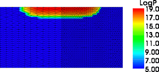
This is how the mb_pn_coarse.vtk mesh looks like. The difference in mesh refinement in the left and right side is intentional to show the effects of improper meshing.

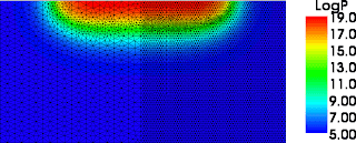
This is how the mb_pn.vtk mesh looks like. Please note how the junction has been refined on the left and right side.

Then we can take both meshes and turn on the diode, bringing the potential of the p contact up to 0.8 V. The computed currents are 3.889297e-02 mA for the coarse mesh and 3.876786e-02 for the fine mesh.


